Power Semiconductor Devices in Power Electronics
Power electronics refers to control and conversion of electrical power by power semiconductor devices whereby these devices operate as switches.
Power electronics run over a broad field of application such as in drives applications, Switch-mode power supply (SMPS), aviation electronics, high frequency inverters and power electronics, Electric power transmission, Automotive electronics, Uninterruptible power supplies (UPS), Alternative power sources controllers etc.
Power Semiconductor Devices (Switches)
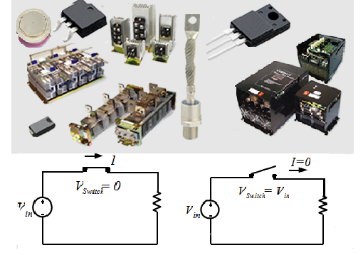
Power switches operates in two states (modes). This is shown in the figure 1 below:
- ON state (Conducting mode): this is when the switch closed.
- OFF state (Blocking state): this is when the switch is opened.
 |
| Figure 1: switching states of a power semiconductor switch |
Note: Power switches don’t operates in linear mode.
Classification of Power Switches
Power switches are classified in three groups. Namely:
- Uncontrolled Switches: Diodes
- Semi-controlled Switches: Thyristor (SCR)
- Fully controlled Switches: Power transistors: e.g. BJT, MOSFET, IGBT, GTO, IGCT etc.
I) UNCONTROLLED SWITCH
Power Diode
It is a two terminal uncontrolled switch formed from P and N type semiconductor materials. When a diode is forward biased, it conducts current (ON state) i.e. a small forward positive voltage (Vf) will turn it ON. The small forward voltage ranges from 0.2-3V depending on the semiconductor material used. When it is reversed biased (a reverse negative voltage from cathode to anode), the diode is OFF.
Diode should not be operated at reverse voltage greater than break down voltage (Vbr). If the reverse voltage is greater than Vbr, then the diode is destroyed.
 |
| Figure 2: Power diode (a) Symbol (b) I-V Characteristics (c) Ideal characteristics |
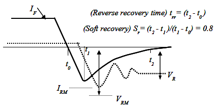
Reverse Recovery of diode
When a diode is switches quickly from forward to reverse bias, it continues to conduct due to the minority charge carriers which remains in the p-n junction. So the time required for the minority carriers to recombine with opposite charge and neutralise is called the reverse recovery time (trr). This effect increases switching losses, increase in voltage rating, over-voltage (spikes) in inductive loads. |
 |
| Figure 3: Reverse Recovery of diode |
Types of Power diodes
i) general purpose :
- Large trr about 25us (very slow response)
- Very high current ratings (up to 5kA) and voltage ratings(5kV)
- Used in line-frequency (50/60Hz) applications such as rectifiers
ii) Fast recovery
- Very low trr (<1us).
- Power levels at several hundred volts and several hundred amps
- Used in high frequency circuits
iii) Schottky
- Limited blocking voltage (50-100V)
- Used in low voltage, high current application such as switched mode power supplies (SMPS).
II) UNCONTROLLED SWITCH
a) Thyristor (SCR)
A Thyristor famously known as Silicon Control Rectifier is a three terminal, four layer solid state semiconductor device (e.g. P-N-P-N structure) and can handle high currents and voltages with better switching speed and improved breakdown voltage.
Thyristors acts as bistable switches. It conducts (ON) when triggered by a current pulse on the gate and OFF only if the current is too low or when triggered OFF.
Conditions in turning ON a Thyristor
1. The thyristor must be forward biased, i.e. the anode should be more positive than the cathode.
2. The thyristor should be triggered with a positive gate current i.e. A positive gate current (Ig) should be applied at the gate.
3. The current through the thyristor should be more than the latching current (a threshold current to turn ON the thyristor).
Once conducting, the anode current is LATCHED (continuously flowing) and so, the gate signal can be removed without turning it OFF.
In reverse -biased mode, the SCR behaves like a diode. It conducts a small leakage current which is almost dependent of the voltage, but increases with temperature. When the peak reverse voltage is exceeded, avalanche breakdown occurs, and the large current will flow.
 |
| Figure 4: Symbol and IV and ideal characteristics of a thyristor |
Latching Current: This is the minimum current required to turn on the SCR device and convert it from the Forward Blocking State to the ON State.
Holding Current: This is the minimum forward current flowing through the thyristor in the absence of the gate triggering pulse.
Forward Breakover Voltage: This is the forward voltage required to be applied across the thyristor to turn it ON without the gate signal application. If the forward breakover voltage (Vbo) is exceeded, the SCR “self-triggers” into the conducting state.
Max Reverse Voltage: This is the maximum reverse voltage to be applied across the thyristor before the reverse avalanche occurs.
Conduction Region: Region where the thyristor is operating in its ON state.
Forward Blocking Region: Region where the thyristor is forward biased but not yet triggered or the voltage didn’t reach the forward breakover voltage.
Reverse Region: consists of the reverse blocking region and the reverse avalanche region similar to the diode characteristic.
Thyristor turn off
The process of turning OFF SCR is defined as "Commutation". Thyristor cannot be turned off by applying negative gate current. It can only be turned off if the current I through it goes negative (reverse). In all commutation techniques, a reverse voltage is applied across the thyristor during the turn OFF process.
III) CONTROLLED SWITCHES
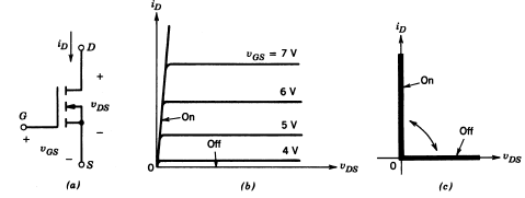
These are switches that can be turned ON and OFF by relatively very small control signals. They operate in SATURATION and CUT-OFF modes only. E.g. Bipolar junction transistors (BJT), Metal oxide silicon field effect transistor (MOSFET), Insulated gate bipolar transistors (IGBT), Gate turn-off thyristors (GTO). Emerging (new) devices: Gate controlled thyristors (GCT).
No “linear region” operation is allowed due to excessive power loss. In general, power transistors do not operate in latched mode.
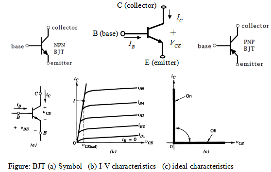
a) Bipolar Junction Transistor (BJT)
 |
| Figure 5: Symbol, IV and ideal characteristics of BJT |
D) Insulated Gate Bipolar Junction Transistor (IGBT)
Combination of BJT and MOSFET characteristics.
 |
| Figure 8: Symbol, IV and transfer characteristics of IGBT |
E) MCT (MOSFET Controlled Thyristor)
F) TRIAC (Triode on Alternating Current)

