PAST GCE QUESTIONS TVE FOR POWER ELECTRONICS
CAMEROON GENERAL CERTIFICATE OF EDUCATION BOARD
Technical and Vocational Education Examinations
Electrical Power Systems EPS (F3)
Note here that the years will not be disclosed. These are the most recent years past questions.
SETTINGS 1
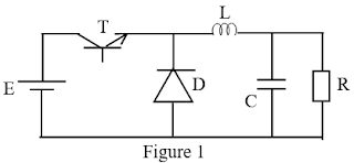
1. The circuit of figure 1 can be referred to as that of
|
A |
voltage step down |
|
B |
current step down |
|
C |
voltage step up |
|
D |
current step up |
2. DIACs are
specifically designed to trigger;
|
A |
TRIACs |
|
B |
Thyristors |
|
C |
GTO |
|
D |
TRIACs and Thyristors |
_______________________________________________
3. A thyristor can be;
|
A |
Turned ON by applying a gate pulse and turned OFF only when current
becomes zero |
|
B |
Turned ON and turned OFF by applying gate pulse |
|
C |
Turned ON by applying a gate pulse and turned OFF by removing the gate
pulse |
|
D |
Turned ON by making current non zero and turned OFF by making current
zero |
_______________________________________________
4. If the firing angle of a rectifier becomes negative
then, the rectifier begins to work as;
|
A |
A negative Rectifier |
|
B |
An inverter |
|
C |
A chopper |
|
D |
A regulator |
_______________________________________________
|
A |
The all
thyristor bridge has a better power factor |
|
B |
The all
thyristor bridge is asymmetrical |
|
C |
The all
thyristor bridge is uncontrollable |
|
D |
The all
thyristor bridge can control power consumed by a load |
_______________________________________________
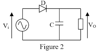
6. In the filtered half-wave rectification circuit, the
minimum peak inverse voltage (VRM) rating of the diode should
be _______ the peak voltage of the source.
|
A |
equal to |
|
B |
2 times |
|
C |
√2 times |
|
D |
0.5 time |
|
A |
Minimize
variations in a.c. input signal |
|
B |
Suppress
harmonics rectified output |
|
C |
Remove ripples
from the rectifier output |
|
D |
Stabilize DC
output voltage |
_______________________________________________
|
A |
Half wave voltage doubler |
|
B |
Full wave voltage doubler |
|
C |
Full wave bridge circuit |
|
D |
Voltage quadrupler |
_______________________________________________
|
A |
Above 20KHz |
|
B |
Above 1000KHz |
|
C |
Less than 10Hz |
|
D |
Equal to 50Hz |
_______________________________________________
10. The role of the diode in the chopper circuit of figure 3 is to overcome:
|
A |
Current variation frequency |
|
B |
Rapid frequency change |
|
C |
Voltage surge during closing
and opening of H |
|
D |
Voltage drop |
_______________________________________________
11. Silicon is preferred
for the manufacturing of semi-conductor components because it
|
A |
Is relatively cheap |
|
B |
Needs lower doping level |
|
C |
Has higher temperature and current capacity |
|
D |
Has lower breakdown voltage |
_______________________________________________
12. Avalanche breakdown is
primarily dependent on the phenomenon of
|
A |
Collision |
|
B |
Doping |
|
C |
Ionization |
|
D |
Recombination |
_______________________________________________
13. The output of a half
wave rectifier is suitable only for
|
A |
Charging of car radios |
|
B |
Running of ac motors |
|
C |
Charging batteries |
|
D |
Running tape recorders |
_______________________________________________
14. 14. Which of the following
approximations is often used in electronics circuit?
|
A |
Ic ≈ Ie |
|
B |
Ib ≈ Ic |
|
C |
Ib ≈ Ie |
|
D |
Ie ≈ Ic + Ib |
_______________________________________________
15. In
a BJT, largest current flow occurs
|
A |
In the emitter |
|
B |
In the collector |
|
C |
In the base |
|
D |
Through CB junction |
_______________________________________________
16. Improper
biasing of a transistor circuit leads to
|
A |
Excessive heat production at collector terminal |
|
B |
Distortion in output signal |
|
C |
Faulty location of load line |
|
D |
Heavy loading of emitter terminal. |
_______________________________________________
17. A
FET consist of a
|
A |
Source |
|
B |
Drain |
|
C |
Gate |
|
D |
All of the above |
_______________________________________________
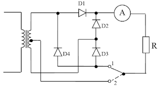
18. Consider figure 4, the period of the load voltage (VL) is ;
|
A |
D1 and D3 conducts |
|
B |
D2 and D4 conducts |
|
C |
D1 conducts and D3 doesn’t conduct |
|
D |
D1 doesn’t conduct D4 conducts |
_______________________________________________
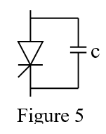
19. The circuit of figure 5 protects the thyristor against:
|
A |
Variation in current |
|
B |
Variation in voltage |
|
C |
Variation temperature |
|
D |
Against overvoltage |
_______________________________________________
20. The ripple factor of a bridge rectifier is
|
A |
0.406 |
|
B |
0.812 |
|
C |
1.21 |
|
D |
1.11 |
_______________________________________________
21. A rectifier circuit with four
diodes is
|
A |
Full-wave center tapped
rectifier |
|
B |
Half wave rectifier |
|
C |
Full wave bridge rectifier |
|
D |
Half-wave center tapped
rectifier |
_______________________________________________
22. During thyristor
application(s), its firing conditions are or is given by
|
A |
VAK less than
zero |
|
B |
iG less than zero |
|
C |
VAK and iG
less than zero |
|
D |
VAK and iG
greater than zero |
_______________________________________________
23. For a non controlled
rectification of acronym PD3 has how many diodes?
|
A |
6 |
|
B |
4 and a thyristor |
|
C |
4 |
|
D |
3 |
_______________________________________________
24. Consider the three phase half wave rectification chronograms from an oscilloscope of load R of figure 6. During manipulation of the Oscilloscope, it was regulated to 5v/division. What is the maximum value of each line voltage?
|
A |
30V |
|
B |
30√3V |
|
C |
60V |
|
D |
60√3V |
_______________________________________________
|
A |
an ac/dc converter |
|
B |
an ac/ac converter |
|
C |
a dc/ac converter |
|
D |
a dc/dc converter |
_______________________________________________
|
A |
average value to its r.m.s. value |
|
B |
r.m.s. value to its average value |
|
C |
peak value to r.m.s value |
|
D |
peak value to average value |
_______________________________________________
|
A |
load resistor |
|
B |
current resistor |
|
C |
bleeder resistor |
|
D |
surge resistor |
_______________________________________________
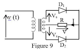
28. In the circuit of figure 7, the reverse voltage across each diode is expressed as
|
A |
|
|
B |
|
|
C |
|
|
D |
2V√2 |
_______________________________________________
|
A |
depletion |
|
B |
saturation |
|
C |
potential
barrier |
|
D |
space charge |
_______________________________________________
|
A |
recombination |
|
B |
ionization |
|
C |
thermal energy |
|
D |
doping |
_______________________________________________
|
A |
VCE
= 0 |
|
B |
VCE
= VCC |
|
C |
VCE
has negative value |
|
D |
IC
is maximum |
_______________________________________________
|
A |
a thyristor |
|
B |
a transformer |
|
C |
a capacitor |
|
D |
a MOSFET |
_______________________________________________
|
A |
cannot be easily destroyed |
|
B |
has a high chopping
frequency |
|
C |
can be triggered by small
gate current |
|
D |
can control heavy power
loads |
_______________________________________________
|
A |
55V |
|
B |
165V |
|
C |
220V |
|
D |
275V |
_______________________________________________
35. What is the duty cycle of a chopper?
|
A |
Ton/Toff |
|
B |
Ton/T |
|
C |
T/Ton |
|
D |
Toff x Ton |
_______________________________________________
36. The expression of the average output voltage for a series
(step down) chopper with an output voltage (E) and duty ratio α is
|
A |
V = E/α |
|
B |
V = αE |
|
C |
V = 2E/α |
|
D |
V= 2E/απ |
_______________________________________________
37. A full wave uncontrolled
rectifier is made of:
|
A |
A bridge of diodes. |
|
B |
One diode |
|
C |
One thyristor |
|
D |
A bridge of thyristors |
_______________________________________________
38. A thyristor is a:
|
A |
Three terminals, four
layers PNPN material. |
|
B |
Three terminals, three
layers PNP material. |
|
C |
Four terminals, four layers
NPNP material. |
|
D |
Three terminals, three
layers NPN material. |
_______________________________________________
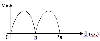
39. The waveform of the figure 8 above is that of the voltage across the resistive load of :
|
A |
Full
wave controlled rectification |
|
B |
A
full wave uncontrolled rectification |
|
C |
Single
phase controlled rectification |
|
D |
Single
phase uncontrolled rectification |
_______________________________________________
40. Which
rectifier requires four diodes?
|
A |
Half wave voltage doubler |
|
B |
Full wave bridge circuit |
|
C |
Full wave voltage doubler |
|
D |
Voltage quadrupler |
_______________________________________________
41. A transistor series
voltage regulator is called emitter follower regulator because the emitter of
the pass transistor follows the ____________ voltage.
|
A |
Base |
|
B |
Input |
|
C |
Output |
|
D |
Collector |
_______________________________________________
42. When BJT is employed
as an amplifier it operates
|
A |
Over the active region |
|
B |
In saturation |
|
C |
Well into saturation |
|
D |
In cut – off |
_______________________________________________
|
A |
20A |
|
B |
(20/π) A |
|
C |
14.14A |
|
D |
(40/π) A |
_______________________________________________
|
A |
arsenic |
|
B |
germanium |
|
C |
boron |
|
D |
silicon |
_______________________________________________
|
A |
2, 8, 4 |
|
B |
2, 10, 2 |
|
C |
2, 7, 5 |
|
D |
2, 4, 8 |
_______________________________________________
|
A |
blocks current |
|
B |
drops a large voltage |
|
C |
has a high resistance |
|
D |
conducts current |
_______________________________________________
|
A |
alternating current to a variable alternating |
|
B |
direct current to a
variable alternating current. |
|
C |
alternating current to a
variable direct current |
|
D |
direct current to a variable direct current |
_______________________________________________
48. When a transistor is fully switched ON, it is said to
be
|
A |
Shorted |
|
B |
Open |
|
C |
Saturated |
|
D |
Cut –
off |
_______________________________________________
49. When a BJT is in saturation
|
A |
Ic = 0 |
|
B |
Vce = 0 |
|
C |
Ib
controls Ic |
|
D |
Vce has
positive value |
_________________________________________
|
A |
60° |
|
B |
90° |
|
C |
30° |
|
D |
45° |
_______________________________________________
NOW GO BACK AND CHECK YOUR WORK
